Semiconductor and Diode Notes: The notes on the topic of semiconductor and Diode concepts are important to understand and memorize to gain an in-depth understanding of this important chapter of Physics. Understanding the core concept of the semiconductor and diode is not only useful in gaining good marks in the board examination but also in cracking competitive exam like NEET UG. To aid students in their preparation journey, our top NEET faculty for Physics at Adda 247 has made a dedicated video to explain all the concepts. The PDF note on this topic has also been created for the convenience of students. They may find both of these resources below in the article.
Semiconductor and Diode Notes
Semiconductor and Diode notes will aid students understand some of the tough concepts given in this chapter. Semiconductor and Diode concept poses many challenges to students due to the practical nature of this chapter. To understand this concept, it is important to study this particular topic from an expert teacher. If you are facing any difficulty understanding this topic, then you are at the right place as our Physics faculty for NEET at Adda 247 have breakdown the tough concepts in a simple manner for students. By going through the video explanation and PDF notes provided in this article, students will surely be a pro in this concept.
Semiconductor
As the name suggests, a semiconductor is a material with some partial conducting ability. A semiconductor does not fall into either the conductor or the insulator classifications. For optimal performance, impurities are typically introduced to the semiconductor. This procedure is often referred to as doping. So, in short, semiconductors are those elements whose properties lies between those of both conductors and insulators. Some examples of semiconductors element are silicon, germanium, etc. Based on the impurities added, semiconductors can be categorized as P Type Semiconductors and N Type Semiconductors.
P Type Semiconductors
An intrinsic semiconductor doped with indium or boron is called a p-type semiconductor. In p-type semiconductors, holes make up the majority of the carriers while the minority carriers are electrons. The hole density is significantly higher than the electron density in a p-type semiconductor. The p-type’s acceptor energy level is located away from the conduction band and near the valency bond.
N Type Semiconductors
An intrinsic semiconductor doped with antimony or phosphorus as an impurity is called an n-type semiconductor. Electrons make up the bulk of charge carriers in n-type semiconductors. In a semiconductor of the n type, holes are minority carriers. The electron density in a semiconductor of the n type is significantly higher than the hole density. The n-type donor energy level is located away from the valency band and near the conduction band.
Intrinsic Semiconductor
Intrinsic semiconductors are defined as semiconductors that are free of impurities and chemically pure. Therefore, rather than the impurities, the characteristics of the material itself control the number of holes and electrons. The number of excited electrons in intrinsic semiconductors, is equal to the number of holes, i.e., n = p. They are also referred to as i-type or undoped semiconductors. I-type semiconductors include, for example, silicon and germanium. These elements have atomic numbers of 14 and 32, respectively, and are members of the IV Group of the periodic table.
Diode
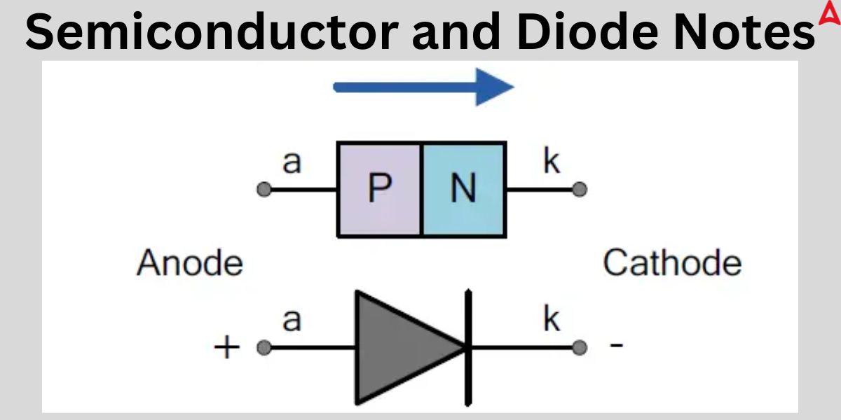
A diode is an electrical component with two terminals that permits current to flow in one direction due to its low resistance to that direction, while its high resistance to the other direction limits the direction in which current can flow. Semiconductor diodes are two-terminal electronic components with metallic contacts at both ends and a p-n junction.
Diode Definition
As per the practical definition, diodes are used to convert AC power to DC and limit voltage in order to safeguard circuits. To maximize the efficiency of diodes, semiconductors such as silicon and germanium are employed. Despite the fact that they only send electricity in one direction, their methods of transmission are different. Diodes come in a variety of forms, and each type has specific uses.
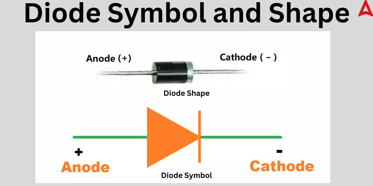
Diode Symbol
Most of the times, the diode is presented in its symbol form. The diode symbol and shape is illustrated below through the diagram.

P-N Junction Diode
An interface or border between the p-type and n-type semiconductor material types inside a semiconductor is known as a P-N junction. Doping is the process that produces the P-N junction in a semiconductor. There are more holes on the semiconductor’s p-side, or positive side, and more electrons on its n-side, or negative side. We employ the doping technique because, as is well known, if we use different semiconductor materials to create a P-N junction, there will be a grain boundary that would prevent electrons from moving from one side to the other by scattering the electrons and holes. The P-N junction diode has two operating regions: N-type and P-type
Depending on the applied voltage, the P-N junction diode has three biasing conditions:
- Zero Bias: The P-N junction diode is not subjected to any external voltage.
- Forward Bias: The voltage potential’s positive terminal is linked to the p-type and its negative terminal to the n-type.
- Reverse Bias: The voltage potential’s positive terminal is connected to the n-type and its negative terminal to the p-type.
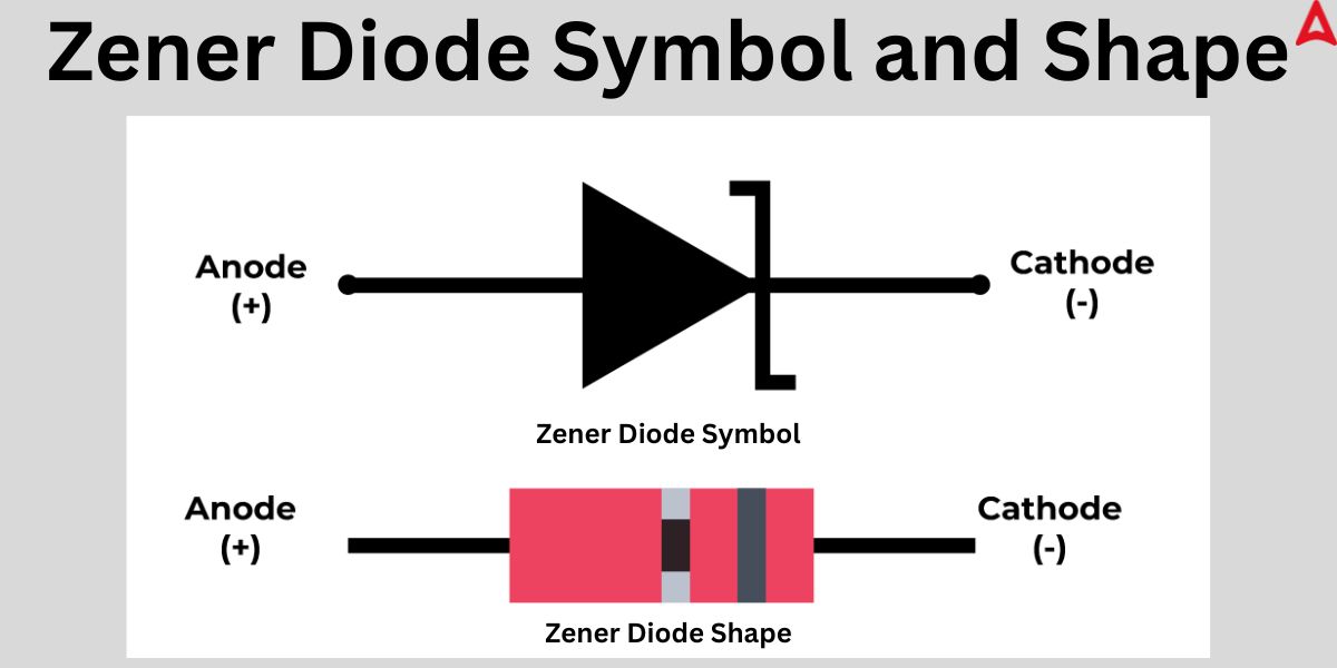
Zener Diode
A breakdown diode, or Zener diode, is a type of highly doped semiconductor device designed to operate in reverse. The junction of a Zener diode breaks down and permits current to flow in the opposite direction when the voltage across its terminals is reversed and rises to the Zener Voltage, sometimes referred to as the knee voltage. One of the main features of Zener diodes is this phenomena, which is referred to as the Zener Effect. The symbol and shape of the Zener Diode is given hereunder.

Semiconductor and Diode Notes PDF for NEET
The semiconductor and diode chapter is a crucial chapter for the Physics section of the NEET exam. Every year, around 3 questions from this chapter are asked in the exam. That is, this chapter holds around 6% of the total weightage for the physics section. Preparing this concept will help students gain 12 crucial marks. As we know, every mark is important in a highly competitive exam like NEET, so, preparing this chapter will prove to be beneficial for students. To help students in this process, our Physics expert for the NEET exam have created the PDF notes for this concept. The below-given notes contain all the detailed information required to master this chapter from the NEET point-of-view.
Semiconductor and Diode Notes PDF for NEET
Semiconductor and Diode NEET Video
The detailed video explanation of all the concepts relevant for the NEET exam on this concept is explained by one of India’s top NEET Physics faculty at Adda 247. The explanation video is unique as it explains many complex details in a simple manner with beautiful illustrations. After going through the video given below and revising the PDF notes, students must be assured of solving any problem related to this chapter.


 Physics Investigatory Project Class 12 T...
 CBSE Class 12 Physics Viva Questions wit...
 Trigonometry Notes for NEET, Download PD...


